MIT Researchers Successfully Integrate 2D Materials Directly on Silicon Circuit

MIT Researchers

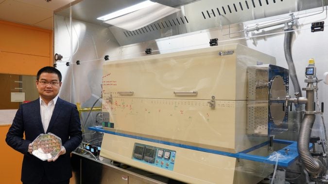
At the MIT.nano facility, researchers demonstrated a newly developed low-temperature process for growing 2D transition metal dichalcogenide (TMD) materials right on an 8-inch wafer. Their successful integration of a 2D material on a silicon wafer can lead to the development of more powerful computer chips potentially benefiting commercial markets.

The post MIT Researchers Successfully Integrate 2D Materials Directly on Silicon Circuit appeared first on HPCwire.


More Related Posts

How pole beans inspired this soft robotic gripper

Illustration of the twining motion in a twining plant (left); Spiral soft...

Unity demos how synthetic data can help robots learn

Unity is showcasing how its AI and machine learning capabilities could benefit...

Pawsey Unveils Fastest Supercomputer in the Southern Hemisphere

The first phase of what will be the fastest public research supercomputer...

Home

Highly Niched Headhunters Specialized in Physical AI/Robotics, High-Performance Computing, Unmanned/Autonomous Systems, Defense Technology and Energy.

Specializations

We recruit across complex engineering markets where understanding the technology is critical to finding the right talent.

How We Work

Overview of how PACE partners with teams: Our process, what clients get, and why PACE is different.

About Us

PACE’s story, values, and culture define how we operate and who we are.

News & Insights

Stay up to date on industry trends.

Contact

All the information needed for anyone interested in contacting us.